

OFC 2025 made one thing clear: The transition to Co-Packaged Optics (CPO) switches in data centres is inevitable, driven primarily by the power savings they offer.
From Jensen Huang showcasing CPO switches at GTC 2025 to a wide range of vendors demonstrating optical engines integrated inside ASIC packages at OFC 2025, CPOs are everywhere.
However, it’s worth noting that Andy Bechtolsheim, co-founder of Arista and a long-standing visionary in data centre networking, has not yet changed his stance. At OFC 2025, he continued to advocate for Linear Pluggable Optics (LPOs) as the better alternative. LPOs, which remove onboard digital signal processors, consume significantly less power than traditional pluggable optics, typically 30 to 50% less. Check out my post for more details.
Andy’s main argument is that the power efficiency of LPOs and CPOs is roughly comparable, at least for the 1600G generation. So why embrace the added complexity of CPO? However, at these higher SerDes speeds, LPOs face challenges with insertion loss in the electrical channels between the ASIC and front-panel optics. Andy believes this can be mitigated using flyover cables with near-package connectors in the 1600G generation.
His concerns around CPOs include the loss of configurability, since all ports must use the same optics type, and the difficulties in mixing and matching optics types. He also points to potential vendor interoperability issues and serviceability challenges. Optical modules are known to experience both hard and soft failures. Even with high-quality optics, hard failure rates are around 100 FIT, and soft failures — often caused by dust in the connectors — are more frequent. With CPO, inspecting or replacing faulty optics takes much longer. Worse, a failed optical port embedded in the package means reduced switch throughput, with no easy replacement.
These concerns aren’t new, but the industry has made significant strides in the last two years. CPO technologies are now far more reliable. Looking ahead to the 400 g-per-lane SerDes generation, CPO may become the only viable option. At such speeds, even the best PCB traces or flyover cables may introduce too much insertion loss. That’s when transitioning to optical signalling within the package itself becomes essential.
So, if the shift is inevitable, why not embrace CPO earlier and help shape its evolution? It will be interesting to see how long Arista holds out before adopting CPO for its shallow-buffer switch line!
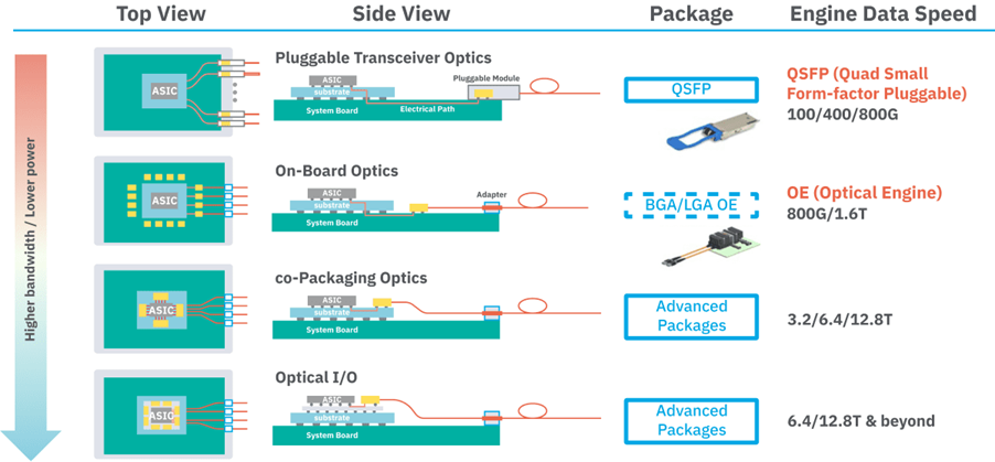
CPO integration
The optical engine of a transceiver — whether co-packaged or part of a pluggable module — typically includes an electronic integrated circuit (EIC) and photonic integrated circuits (PICs). Refer to my post from almost three years ago to understand the internals of the PIC.
There are two main ways to integrate these optical engines inside the ASIC package containing the switch or XPU cores.
Silicon interposer approach
The core die and the Electronic Integrated Circuit (EIC) can be co-located on a silicon interposer (or connected via silicon bridges like Intel’s EMIB), and the Photonic Integrated Circuit (PIC) is either 3d-stacked on top of the EIC or placed in the organic substrate. When the PIC/EIC stacks are next to the core die in the silicon interposer, they are also referred to as optical I/Os.
The goal is to shorten and improve the electrical link between the core die and the optical engine by leveraging high-density D2D links and the interposer routing. This interposer approach allows multiple optical chiplets to be placed closer together to the main die, thus yielding a smaller package.
However, co-locating the high-power EICs and the core dies on an interposer can complicate thermal management. Moreover, if the PIC is stacked on the EIC, dissipating heat from the EIC is harder. A large silicon interposer adds cost and complexity to packaging. The interposer size constrains how many optical modules can surround the ASIC. To increase the bandwidth without increasing the complexity or cost, the optical engine will be required to have a much higher bandwidth density.
Organic substrate approach
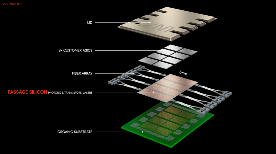
The second approach keeps the optical engines on the organic substrate inside the ASIC package (not on a silicon interposer). The PIC and EIC are assembled together (usually stacked on top of each other with PIC at the bottom) to form a compact optical engine module that is then mounted on the organic substrate surrounding the main die. Core die communicates with the EIC through Serializer/Deserializer (SerDes) interfaces, which typically have 500 to 1,000Gbps/mm bandwidth density in the latest process nodes. That means, a core-die with 625sq mm area (25mm on each side) could send about 100Tbps of bandwidth out of the die to the optical engines. To escape >100Tbps bandwidth, we typically need multiple core dies inside the package.
This approach allows the optical engines to be spaced apart on the substrate and somewhat relaxes the optical bandwidth density requirement for each engine. Since the engines are spread farther from the main die, this helps with thermal isolation. Each optical engine can potentially have its own mini heat sink or be spaced such that airflow or a cold plate can reach it. Importantly, stacking the PIC and EIC with the PIC at the bottom (closest to the substrate) gives better heat dissipation and signal performance than the reverse.
Without large interposer constraints, the package can be made larger (without significantly increasing the cost) to accommodate more engines if needed. The assembly process, while still complex, is modular. The optical engines can be tested stand-alone before mounting them on organic substrates. This is the popular approach for integrating the CPOs.
What is bandwidth density?
Not all CPO solutions are identical. The final goal of any CPO solution is to achieve high bandwidth density with the lowest power possible. This raises the next question: What exactly is bandwidth density?
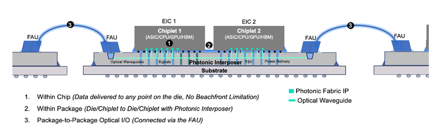
In the context of CPOs and optical I/O, bandwidth density — often referred to as beachfront density or shoreline density — describes the amount of data, typically in terabits per second (Tbps), that can be delivered per millimetre along the edge where optical interfaces are integrated. Note that this metric is not measured at the front-panel connector level, but rather at the edge of the ASIC die or the edge of a photonic chiplet or optical engine co-packaged with the ASIC. These are the physical boundaries within the package where optical fibres or waveguides are coupled.
Industry sources consistently use this definition, often expressing bandwidth density in units like Tbps/mm or fibres/mm, depending on whether the emphasis is on throughput or physical channel count. A higher beachfront density means more optical bandwidth can escape the chip without increasing its footprint. Improving beachfront density is vital to meeting the exploding bandwidth demands in data centres and HPC systems.
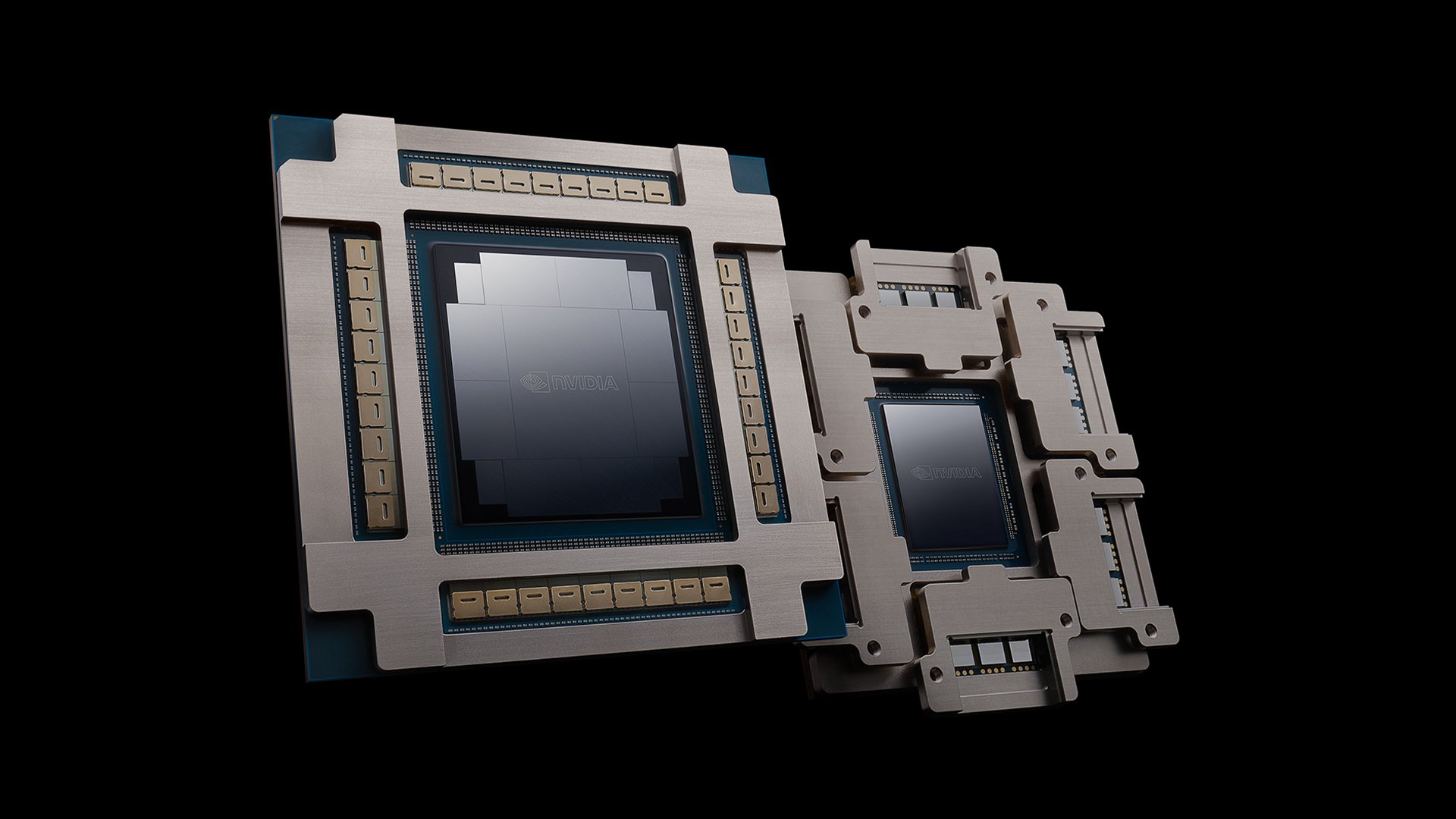
Comparing implementations: Broadcom vs Nvidia
Now, to understand co-packaged optics, let’s examine Broadcom and Nvidia’s CPO offerings more deeply.
Package bandwidth
Broadcom unveiled its Bailly CPO switch last year. The switch is based on the Tomohawk-5 ASIC, with eight 6.4Tbps optical engines integrated inside the package. The total off-package optical bandwidth is 51.2Tb/s (64 x 800Gbps or 128 x 400Gbps)
We can expect the next-gen 102.4Tbps CPO switch to use an evolved CPO architecture, with improved silicon photonic engines (12.8Tbps or even higher bandwidth per engine) surrounding the Tomahawk-6 die. These ~100Tbps switches may be available in the second half of this year.
Broadcom builds chips that switch vendors can use to build systems. A few companies are in various stages of development (or early sampling) of switches built using the Bailly switches. In all these switch offerings, a single Baily chip (with 128 x 400G ports in the front panel) is used to build standalone systems.
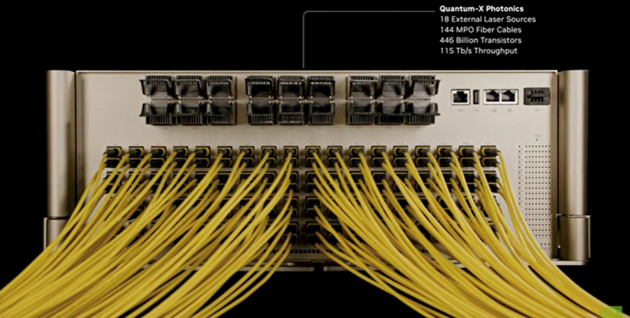
NVIDIA’s co-packaged optics platform, unveiled at GTC 2025, targets even higher totals, scaling to 100Tb/s and beyond.
The Quantum-X InfiniBand switch system will have:
- 144 ports of 800Gb/s (or 576 x 200Gbps) totalling 115.2Tbps bandwidth.
- Four Quantum-X CPO packages using the Quantum X800 ASIC. Each package has 28.8Tbps of bandwidth (144 x 200Gbps or 36 x 800Gbps).
- If we were to get 115.2Tbps of non-blocking switching capacity with 28.8Tbps switches, we would need a lot more than four switches in a Clos configuration. Since there seems to be only four switches, it looks like this is not a true 115.2Tbps switch. Any comments?
- It is expected to be available by late 2025.
The Spectrum-X Photonics Ethernet switch family will have
- 128 ports of 800G (or 512 ports of 200G), giving 102.4Tb/s. This likely will have two Spectrum-X CPO packages, each with 51.2Tbps (64 x 800Gbps or 256 x 200Gbps) bandwidth.
- A larger configuration with 512 ports of 800G (409.6Tb/s) will also be available, likely with 4 x CPO packages.
- Similar to Quantum, unless more switches are used for chip-to-chip connectivity inside the switch chassis, these are not true 102.4T or 409.6Tbps switches.
- These systems are expected to be available in 2026.
So, in terms of capacity, Broadcom has a 51.2T solution today, aligning with current network needs (800G Ethernet era with 100G SerDes), with 100Tbps in the 2025 roadmap, while NVIDIA is leapfrogging to 100 to 400T to meet future million-GPU cluster demands with 200G SerDes. NVIDIA’s larger bandwidth numbers reflect a more aggressive architectural approach with a focus on large-scale integration (using multiple photonic switch chips inside a system) to realize higher radix switches.
Optical engines
The Broadcom Bailly chip integrates 6.4Tbps silicon-photonics-based optical engines inside the ASIC package. These high-density edge-mounted optical engines directly interface with the core die through short, chip-to-chip connections through the organic substrate. This tight integration yields a simpler physical layout.
NVIDIA’s Spectrum-X (Ethernet) and Quantum-X (InfiniBand) photonic switches also incorporate multiple 1.6Tbps silicon-photonics-based photonic engines. Each photonic engine is built with TSMC’s COUPE™ process that stacks an electronic die (EIC) atop a photonics die. Three of these engines are clustered into detachable optical sub-assemblies (OSAs) with 4.8Tbps of throughput. This means the optical engines (and their fibre interfaces) are on replaceable modules that mate with the switch substrate, rather than being permanently bonded like Broadcom’s!
Nvidia’s packaging is thus a bit more complex. It uses advanced 2.5d/3d integration (TSMC System on Integrated Chips (SoIC) stacking for the engine dies) and a modular attachment system for the optical parts. This addresses the concern of serviceability to some extent. If a plug-in module is found faulty during manufacturing testing, it can be replaced with a different module.
In the Quantum-X CPO switch, each ASIC package consists of the Quantum X800 28.8Tbps switch ASIC core with six OSA plug-in modules connected to the main package.
In summary, Broadcom’s solution is a single-package switch with optics embedded, whereas NVIDIA features a novel package with removable photonics modules.
The spectrum-X CPO package gives us more insights into the chiplet organization. It seems to have the main core switch die along with eight I/O dies closely integrated together (with die-to-die interfaces) and the photonic engines (36 of them) surrounding them in the organic substrate. Whether these photonic engines will be part of detachable OSAs is not known.
Fibre coupling
Broadcom’s CPO switch uses edge-coupled fibre attachments from the optical engines to achieve high beachfront density. Each optical engine PIC has waveguides on-chip that carry optical signals. These waveguides end at the edge of the photonic chiplet. Optical fibres are precisely aligned and permanently bonded (typically using epoxy) to these waveguide facets.
Broadcom has developed a highly automated, high-density fibre attach process, aligning many fibre cores precisely to the optical chiplet edges. This edge coupling scheme allows a large number of optical channels to escape the package in a compact footprint.
In their first generation of CPO, Broadcom seems to be using 400 G-FR4 to have four 100G channels on a single fibre using Coarse Wavelength Division Multiplexing (CWDM). With this, each optical engine has 16 fibre-pairs (tx+rx = pair) to handle 6.4T throughput. However, Broadcom may be working on a new version of the chip with 64 fibre-pairs (each carrying 100Gbps) to enable larger radix switches (with 512 x 100G ports).
The short fibres emerging directly from the optical engine are called ‘fibre pigtails’. The fibre pigtails exiting the optical engines must be routed to the front panel connectors. However, these are short and fragile and can’t be routed directly to the front panel. The fibre pigtails from the ASIC usually connect internally (inside the switch box) via connectors to longer, more robust fibres running to the front panel.
Nvidia’s Quantum-X InfiniBand switch package has 324 optical connections emanating from each CPO package. To support 144 x 200Gbps, 144 fibre pairs (288 fibres) would be needed. The remaining 36 are for laser connections to the ASIC — each of the 18 photonic engines gets two laser inputs.
Four fibre pairs (4 × 200Gbps) each are grouped together (DR4) and terminated into a single Multi-fibre Push On (MPO) connector at the front panel. Thus, the switch system with four CPO packages has 144 MPOs at the front panel.
While details of the coupling method are not fully public, it’s likely that NVIDIA may also be using edge coupling on the photonic engines.
In summary, both Broadcom and NVIDIA had to solve fibre coupling at a massive scale. While Broadcom relies on WDM to reduce the fibre count in the first version of the CPO switch, Nvidia does not seem to have WDM based on the fibre count it showed in the GTC presentation.
Laser integration
One of the biggest considerations in CPO design is how to handle the lasers that provide the light source for the modulators inside the optical engines.
Both Broadcom and Nvidia designs keep all high-power lasers off the main switch package, instead using external, pluggable laser modules (External Laser Source (ELS)). These modules can be plugged into the front panel Lucent Connector (LC) ports that accept hot-swappable laser cartridges.
Fibre patch cords deliver the continuous-wave light from these laser modules into the co-packaged optical engines. This strategy keeps the CPO’s power low and improves its reliability. Lasers may degrade faster than other components, so external lasers can be easily replaced without disturbing the switch ASIC.
The Bailly switch uses 16 efficient pluggable laser modules, two modules per 6.4Tbps optical engine.
NVIDIA’s solution goes further by drastically reducing the total number of laser sources needed. In the Quantum-X photonic switch system, only 18 laser modules connected at the front panel supply light to all 144 x 800G optical channels. Each module has eight integrated lasers and supplies the light source for eight 1.6Tbps photonic engines. Thus, the NVIDIA architecture uses 4× fewer pluggable laser modules (when counting modules per unit bandwidth) than the Broadcom approach.
Fewer lasers mean fewer components to cool and monitor, but it also means that if a laser module fails, more channels could be affected.
Modulators
Modulators are components inside the optical engine that convert electrical signals into light signals. They take the steady light from a laser and imprint high-speed data onto it by turning the light into intensity or phase-modulated optical data streams. Understanding how these modulators work is a deep technical topic that is beyond my domain expertise.
Without going into too many technical details, the high-level summary is that Broadcom most probably uses a Mach-Zehnder Modulator (MZM). These types of modulators are less sensitive to laser instability and have better tolerance to temperature variations. However, they have higher power and a larger footprint (area). While MZMs are good for 100Gbps signalling, they hit density and power limits when scaled to ~200G lanes and hundreds of Tbps CPO packages.
That is probably the reason Nvidia CPO solution picked Micro-Ring Resonator Modulator (MRM), which has a smaller footprint (scales really well) and needs a lower drive voltage, and hence less power. These modulators also support WDM natively. Each ring targets one wavelength, perfect for 8 to 16λ per fibre systems. But these modulators need more tuning (due to their thermal sensitivity) and robust DSP logic to reduce the crosstalk. Nvidia’s choice of MRM shows their aggressive approach to power savings in their CPO solutions. MRMs consume ~1 to 2pJ/bit, compared to 5 to 10pJ/bit for MZMs.
Wave Division Multiplexing
Broadcom uses coarse WDM with a 4λ × 100G configuration to carry 400G per fibre. Their documentation does not explain how the 800Gbps port configuration is achieved. It may involve non-standard configurations like dual 400G FR4 links aggregated together. Or, they could be developing a new version of the CPO switch that can support DR links (Direct Reach, no WDM, each fibre carries 100G).
NVIDIA’s Quantum-X does not seem to have WDM support based on the number of fibre pairs from each CPO package, which matches the number of 200G ports.
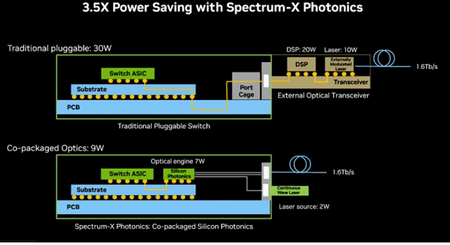
Power efficiency and cooling
One primary motivation for co-packaged optics is improving power efficiency. Both Broadcom and NVIDIA report dramatic power-per-bit savings over traditional pluggable transceivers.
Broadcom claims roughly 5.5W per 800Gb/s port for its CPOs, versus ~15W for an equivalent pluggable module. This 3× reduction means a fully loaded 64-port (800G each) switch can save on the order of hundreds of watts. This 5.5W power translates to 6–7pJ/bit for the optical links, which is class-leading for 2024.
Cooling such a system is easier than cooling an equivalent switch with dozens of 15W pluggable devices. Still, a 51.2T CPO switch will dissipate significant heat with its concentrated power density on the ASIC package, which would require cold-plated liquid cooling. However, its units likely can work with high-performance air cooling as well.
NVIDIA likewise touts major efficiency gains: 3.5× more power-efficient network links with its silicon photonics switches, by using micro-ring modulators and far fewer lasers. Similar to Broadcom, these switches would need liquid cooling to efficiently remove the heat from the ASIC packages. In fact, the Quantum-X CPO presentation at GTC does show cold-plate liquid cooling for the switch ASICs.
In short, both solutions yield much lower pJ/bit, making ultra-high-bandwidth networking more sustainable.
Breaking the bandwidth wall — future directions
Vertical coupling
Traditional optical engines often use edge coupling, which aligns fibres to waveguide facets at the chip edge. Edge coupling with V-groove fibre arrays is a known method for precisely spacing fibres (often 50–250µm apart) and passively aligning them to waveguides.
Edge couplers can offer low insertion loss and are straightforward to attach to the fibre ribbons. However, they consume significant edge length because the fibres must be laid out side by side with minimum spacing.
Another approach, vertical coupling, uses on-chip diffractive grating couplers or mirrors to couple light out of the top surface of the chip. This allows optical I/O to be placed across the chip area, not just the perimeter. Vertical couplers plus microlens arrays can achieve dense coupling and have the flexibility of placement anywhere above the photonic die. The trade-off is typically higher loss and alignment complexity when scaling to many fibres.
While edge coupling is currently prevalent (due to maturity and efficiency), vertical coupling is being actively explored in research labs and by some companies to overcome the edge-length constraints.
Multi-core fibres and fibre pitch reduction
If each fibre can carry multiple cores (light paths), the number of fibre objects at the edge can be reduced for a given number of channels. Multi-core fibre (MCF) packs several independent cores within one fibre cladding. This efficiently uses the limited beachfront area by stacking channels in one fibre cross-section. For example, a 4-core fibre could quadruple the channels per fibre, immediately boosting edge channel density 4×. While not yet standard in commercial CPO products, it’s considered ‘an attractive solution’ to the limited photonic beachfront.
The downside of MCF is that if the systems require a larger radix of lower-bandwidth ports going to different servers / Network Interface Cards (NICs), aggregating more bandwidth inside a single fibre is not a good idea.
Another way to increase the fibre density is to reduce the pitch. Standard SMF ribbon pitch is around 250um. By using thinner fibres or removing buffer, pitches of 50µm or even less can be achieved. IBM demonstrated 50µm fibre channel pitch in a reliable assembly and even 18µm pitch with custom polymer fibres in the lab. Such small pitches greatly increase ‘fibres per mm’ and enable larger bandwidth out of ASIC packages.
Advanced couplers, lenses, and attachment methods
As fibre pitch shrinks and counts rise, alignment tolerance becomes a challenge. Techniques such as grating couplers with micro-lens arrays are being developed to ease alignment restrictions. This could enable very dense, 3d-stacked fibre connector arrays on top of a photonic chip.
Fiber attachment methods are also evolving. Many CPO implementations today still rely on the precision placement of fibre arrays and then securing them with epoxy. Moving forward, expect to see more connectorized solutions, such as Nvidia’s detachable modules or startups providing ‘plug-and-play’ optical socket chiplets.
WDM is the current method to get more channels per fibre; vertical coupling, multi-core fibres, dense fibres, and novel attachments are emerging to further boost beachfront density. Each technique addresses a different aspect (geometric density vs per-fibre capacity vs alignment). The next-gen CPO implementations are exploring using multiple methods to enhance the total off-chip bandwidth within a given edge length.
CPO deployment hurdles
The primary hurdles are less about the core technology itself and more about the impact CPO has on the established ecosystem and operational models:
- Ecosystem Disruption: CPO fundamentally changes the supply chain. Instead of purchasing interchangeable pluggable modules from multiple vendors, customers have to source integrated CPO switches or servers from a single system vendor or a tightly coupled partnership. This reduces sourcing flexibility and increases vendor lock-in.
- Operational Complexity: Field replacement and failure management become more complex. A failure in an optical engine might require replacing an entire CPO switch line card or server board rather than just swapping a pluggable module. Developing robust testing, diagnostics, and repair strategies for CPO systems at scale is a major undertaking.
- Reliability Proof: While CPO potentially offers higher reliability by eliminating the pluggable connector interface (a common failure point), this needs to be proven through large-scale, long-term deployments. Data on CPO reliability is starting to emerge, but more validation is needed.
- Cost: At present, CPO does not have a significant cost advantage over high-volume pluggable optics. As the volumes pick up, this equation should change.
- Thermal Management: Integrating heat-sensitive optical components inside ASIC packages poses significant thermal challenges, and liquid cooling is a must.
Given these challenges and the rapid maturation of 1.6T pluggable optics, it is unlikely that CPO will see massive volume deployment for scale-out applications in the 200G/lane generation.
However, the industry anticipates seeing ever-larger test deployments of CPO to validate the technology and operational models, potentially paving the way for mass deployment in a subsequent generation.
CPOs for scale-up?
CPOs’ prospects appear brighter for the scale-up use case (intra-rack connectivity). In this scenario, the entire rack solution (including accelerators, switches, and interconnects) is more likely to be sourced from a single vendor (like Nvidia) or a tightly integrated partnership. This simplifies the ecosystem challenges, making CPO integration more straightforward.
At GTC 2025, Jensen Huang unveiled NVL144 (based on Rubin GPU), which continues to use copper cables for NVLink interconnects at 200 Gbps lane speeds. At these rates, the copper cables can be bulky, and cable management could be messy.
Optical backplane/midplane links offer massive improvements in cabling and reach. A single ribbon fibre can carry many wavelengths, replacing dozens of copper cables. This greatly reduces weight and congestion, which is important not just for cooling but also for signal integrity. Optics also allow a chassis to scale in size and create super scale-up clusters across multiple racks without having to keep everything within a few meters.
GPUs and scale-up switches (like NVSwitch) with CPOs for NVLink interconnects enable these optical backplanes. Refer to my post on wide-bus photonic backplane and other trends for optical backplanes.
However, passive copper cables are still great for power, and Nvidia will continue to use copper cables in scale-up systems as long as they can make it work with lower power (even if they have to add retimers in between).
The logical choice for GPUs (or other accelerators) in scale-up systems may be to transition to CPC (Co-Packaged Copper) first. This would eliminate the PCB traces and rely entirely on the flyover copper cables for the backplane connectivity. Any thoughts on the transition to CPOs and optical interconnects at ~400Gbps or above link speeds?
What’s next? Photonic fabrics/interposers?
An alternative to conventional CPO with optical engines on the edges is to use photonic interposers or fabrics that are placed beneath the core dies. Think of this as a 3d stacked configuration where the lasers, waveguides, and optical switching/routing reside in a base layer, on top of which compute or memory chiplets can be mounted. This essentially provides an optical motherboard for chiplets.
Because the photonic interposer can be large (3 to 4x reticle size), it can offer a very long ‘edge’ — a continuous 2D surface for optical I/O. Consequently, the effective bandwidth per mm of edge can be very high compared to what can be achieved with many discrete optical engines placed apart.
Several startups have been actively exploring this over the last few years (I wrote an article about it two years ago), and many demos at OFC 2025 illustrate its feasibility.
The primary challenge with photonic fabrics is that the optical engines in the base layer dissipate a lot of heat, making heat management in this 3d stacked configuration quite challenging. While the demos primarily feature test chips at the top (which only have Serdes and minimal logic), it would be intriguing to see how the thermal management looks in a real 3d photonic-fabric chip, where the core dies and optical base layers consume a large amount of power.
Some start-ups are also investigating photonic fabrics to connect multiple XPUs in a package. When there are many cores inside the package, photonic fabrics could provide connectivity between non-adjacent cores at a much lower latency than the traditional approaches of routing through the organic substrates.
Another application for optical interconnects is connecting XPUs to a pool of memories (high bandwidth memory) housed in separate ASIC packages on the board. Since the latency through the fibre is low, this could enable the disaggregation of memories from the ASICs.
However, electrical-optical-electrical conversions consume significant power for any photonic connectivity. If alternative approaches for ultra-large-scale integration involve multiple ASIC packages and PCB traces, the photonic fabric approach may emerge as a superior solution. All that said, these are longer-term developments.
Today’s focus is on CPO for switches because that’s the immediate pain point. The industry is abuzz with excitement over this. The successful deployment of CPO switches will pave the way (in terms of technology, supply chain, and trust in optics) for extending photonics elsewhere!
Exciting times ahead…
Note: For this primer, I mainly focused on the CPO solutions from Broadcom and Nvidia. However, many vendors offer various components used in CPO and the technology to integrate CPOs in XPUs/switches. This article is more of a technology review and does not intend to cover all the vendors in this ecosystem.
Sharada Yeluri is a Senior Director of Engineering at Juniper Networks, where she is responsible for delivering the Express family of Silicon used in Juniper Networks‘ PTX series routers. She holds 12+ patents in the CPU and networking fields.
Adapted from the original on LinkedIn.
The views expressed by the authors of this blog are their own and do not necessarily reflect the views of APNIC. Please note a Code of Conduct applies to this blog.
Excellent article. I’m used to reading similar, and thinking that the author did not fully comprehend the details. Not so here.
Very informative…. thanks
Excellent. Very informative.
good knowledge